Experiment 7: Boost Converter
Introduction
A boost converter’s output voltage is always higher than the input voltage. Figure 1 shows the schematics of a boost converter. It has a dc input voltage, a transistor working as a switch, an inductor and a capacitor forming a low pass filter to smooth out the output voltage, and a load resistor. The diode provides a path for the inductor current when the switch is opened and is reverse biased when the switch is closed.
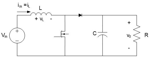
Figure 1. Schematics of a boost converter
When the switch is closed, the diode is reverse biased. The equivalent circuit is shown in Figure 2.
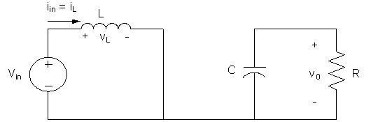
Figure 2. Equivalent circuit when the switch is closed
When the switch is open, the diode is forward biased. The equivalent circuit is shown in Figure 3.
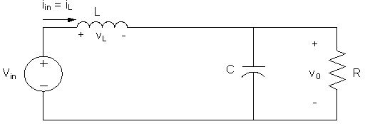
Figure 3. Equivalent circuit when the switch is open
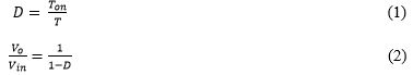
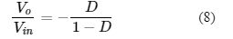
Output voltage of a boost converter is controlled by a pulse width modulated (PWM) signal shown in figure 4. The duty cycle is the ratio between the on time and the switching period shown in (1). By adjusting the duty cycle, we can obtain desired output voltage, which is shown in (2). When D increases, the output voltage increases. When D decreases, the output voltage decreases.
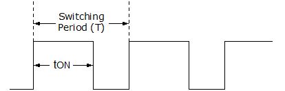
Figure 4. Pulse width modulated (PWM) Signal
If the inductor current is continuous, the boost converter is operating in continuous conduction mode. If the inductor current is reduced to zero, the boost converter is operating in discontinuous mode. We would like to keep the boost converter operating in continuous conduction mode. The minimum inductance to keep the boost converter in continuous conduction mode is the critical inductance. Value of the critical inductance is shown in (3).

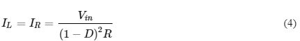
Average inductor current is the same as the average load current in the load resistor. Value of the average inductor current is shown in (4).
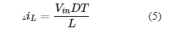
The peak-to-peak inductor current is often a design criterion in the design of a boost converter. It is also called the current ripple. Equation (5) shows the value of the current ripple. The current ripple is inversely proportional to the inductance and the switching frequency. To reduce the current ripple, we can increase the inductance or the switching frequency.
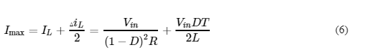
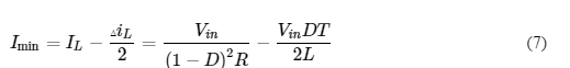
The maximum inductor current is the average inductor current plus half of the current ripple, shown in (6). The minimum inductor current is the average inductor current minus half of the current ripple, shown in (7).
Another basic dc-dc converter is buck-boost converter shown in Figure 5. The output voltage of a buck-boost converter can be either higher or lower than the input voltage. Ratio of the output voltage over the input voltage is shown in (4). If D>0.5, the output voltage is greater than the input voltage. if D < 0.5, the output voltage is less than the input voltage.
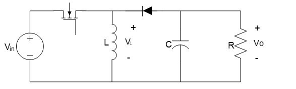
Figure 5. Buck-boost converter
- Characteristics of boost converter
- Capacitor and inductor selection
- Output voltage and current
- Continuous and discontinuous mode
- Power Supply
- Capacitor
- Inductor
- MOSFET
- Diode
- Resistor
-
Make connections of power supply, capacitor, inductor, MOSFET and load resistor to build the boost converter.
Vin = 12 V; D = 40%; C = 2000 μF; L = 1000 μH; R = 50 Ω; f = 20 kHz - Check the circuit connections according to the schematics.
-
Varying duty cycle
- Set the duty cycle at 40%, and switching frequency at 20 kHz.
- Calculate the value of the output voltage.
- Observe and measure the output voltage. Compare with the calculated value.
- Vary the duty cycle from 20% to 80% with the interval of 10%.
- Measure the output voltage VO for each of the duty cycle. Compare the measurement with theoretical calculation.
- How does the output voltage change when the duty cycle increases?
- Set the duty cycle at 40%, and switching frequency at 20 kHz.
- Observe and measure the output current ripple. Compare the measurement with theoretical calculation.
- Increase the switching frequency to 50 kHz. Observe and measure the output current ripple. Compare the measurement with theoretical calculation.
- How does the output current ripple change when the switching frequency increases?
- Set the duty cycle at 40%, and switching frequency at 20 kHz.
- Measure the load current IL and output voltage VO when the load resistance is 10 Ω. Compare the measurement with theoretical calculation.
- Measure the load current IL and output voltage VO when the load resistance is 20 Ω. Compare the measurement with theoretical calculation.
- Schematics for a boost converter
- Show your calculation for output voltage for each duty cycle. Compare with the measurement values and plot the output voltage for each of the duty cycles. Pressing
 on the upper right corner of the waveform will allow you to save the image.
(B) Boost Converter (Switching Frequency)
- Show your calculation for output current for each switching frequency. Compare with the measurement values and plot the output current for each of the duty cycles.
- Show your calculation for output voltage and current for each load resistor. Compare with the measurement values and plot the output voltage and current for each load resistor.
Contact Us
Virtual Renewable Energy Laboratory
Principal Investigator:Liping Guo, Ph.D.
815-753-1350
lguo@niu.edu
Co-Principal Investigator:
Andrew W. Otieno, Ph.D.
815-753-1754
otieno@niu.edu
The project is funded by the
National Science Foundation
Improving Undergraduate STEM Education program (DUE-1712146)
from June 2017 to May 2020.